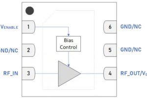
“TCWA1225G offers an input peak power of 46dBm – at 8dB PAR,” the company said. “This has been achieved by adopting Toshiba’s original CMOS process and optimising the internal switching circuitry.”
The process also reduces insertion loss, typically to 0.6dB at 5GHz, it added.
This is at 25°C, where the max value is 0.9dB. Over the full temperature range of -40 to +95ºC, it increases to 0.8dBmax from 0.7 to 3GHz, and 1dBmax from 3 to 5GHz.
50Ω terminated power handling is 24dBm, and the packaged device can handle 1W at 25°C and 0.3W at +95°C.
Operation is from 3 to 3.6V – where it typically draws 50μA (200μA max).
Switching is in 750ns (1.5μs max).
Applications are foreseen inside ‘massive’ MIMO (multiple-input multiple-output) antennas in 5G installations, as well as in industrial equipment and repeaters.
Find the TCWA1225G on this web page