According to the company: “Scalable i.MX 9 families bring together higher performance applications cores, an independent MCU-like real-time domain, state-of-the art security and dedicated multi-sensory data processing engines for graphics, image, display, audio and voice. i.MX 9 integrates hardware neural processing units for acceleration of machine learning applications.”
Arm Ethos U-65 ‘microNPU’ will be included for edge machine learning, and the first chips will be on 16/12nm FinFET processes.
Security will be through a self-contained root-of-trust that the company is branding ‘EdgeLock secure enclave’ and combines secure boot, crypto processing, random number generation, e-fuses and one-time-programmable memory. It provides: “device-wide security intelligence, run-time attestation, silicon root-of-trust, key management, cryptographic services, trust provisioning and a simplified path to certification”, it said.
This security block, i.MX 9 has in common with the new part NXP has announced in detail – i.MX 8ULP with its Azure Sphere-certified cousin i.MX 8ULP-CS.
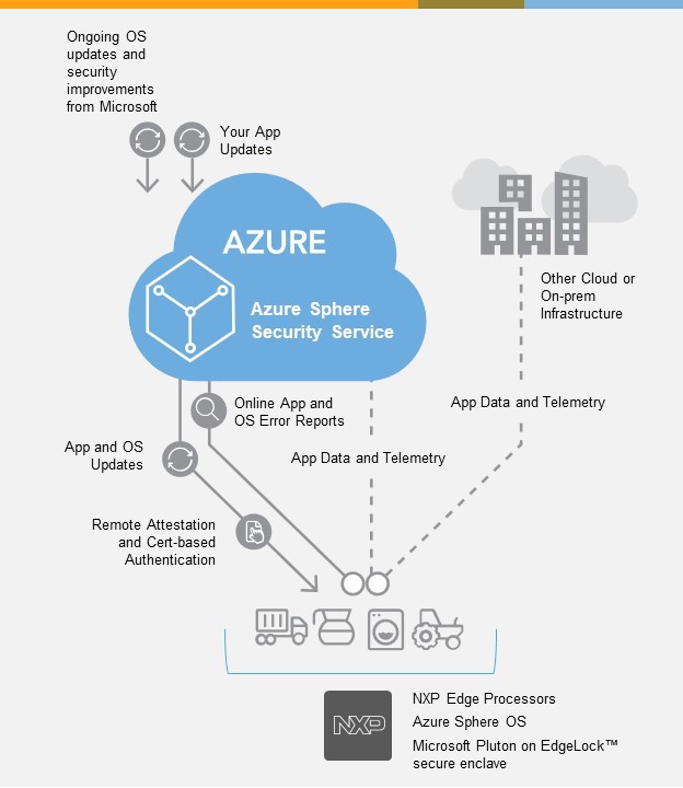
In addition to the secured hardware, Azure Sphere includes the secured Azure Sphere OS, the cloud-based Azure Sphere Security Service, and ongoing OS updates and security improvements for over ten years. “Azure Sphere chip-to-cloud security will be enabled on specific products within the i.MX 9 series, giving developers an even broader set of processor options to implement managed device security across more of their products.”
“i.MX 8ULP-CS with Microsoft Azure Sphere will provide security, productivity, and opportunity for partners,” said Microsoft MD Galen Hunt. “This collaboration is going to empower a whole new class of connected devices supported by ongoing security improvements.”
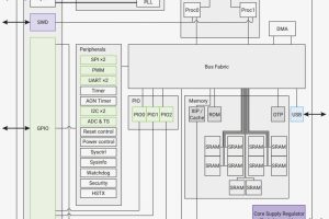
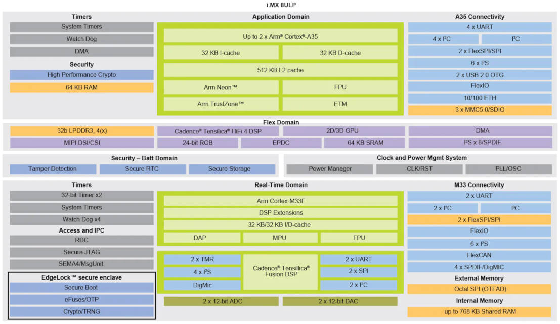
Alongside Edgelock, the i.MX 8ULP processors (see diagram) come with one or two 1GHz Arm Cortex-A35 application processors, plus a 216MHz Cortex-M33 real-time processor and a 600MHz Cadence Tensillica Hifi 4 DSP for audio, voice and machine learning, then a 200MHz Fusion DSP for low-power voice and sensor hub processing. The power management sub-system gets it own Risc-V core too.
There is a 3D graphics processing unit for Open GL ES 3.1, OpenCLTM and Vulkan, plus 2D graphics. These have external access through 1x MIPI DSI (4-lane) with PHY at up to 24bit RGB (DBI/DPI). Colour electronic paper displays can be connected.
Total on-chip SRAM count is 896kbyte, and external memory can include: LPDDR3/LPDDR4/LPDDR4X, SPI-NOR and SPI-NAND.
Other interfaces include: 10/100 Ethernet and FlexCAN, then 1x MIPI CSI (2-lane) with PHY for a display or camera.
Package options are 9.4 x 9.4mm FCBGA or 15 x 15mm MAPBGA. Operation is across -40 to +105°C.
They are built on a 28nm FD-SOI process, and the programmable power management sub-system has access to more than 20 different power modes down to 30μW.