3D integration brings, under a single roof, expertise and equipment addressing the entire 3D integration value chain: technology, circuit architecture, EDA tools, packaging and test. STMicroelectronics (IDM), Mentor (EDA), a Siemens business, EVG and SET (equipment suppliers), and CEA-Leti (RTO) are the current members of the consortium.
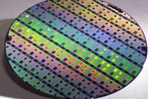
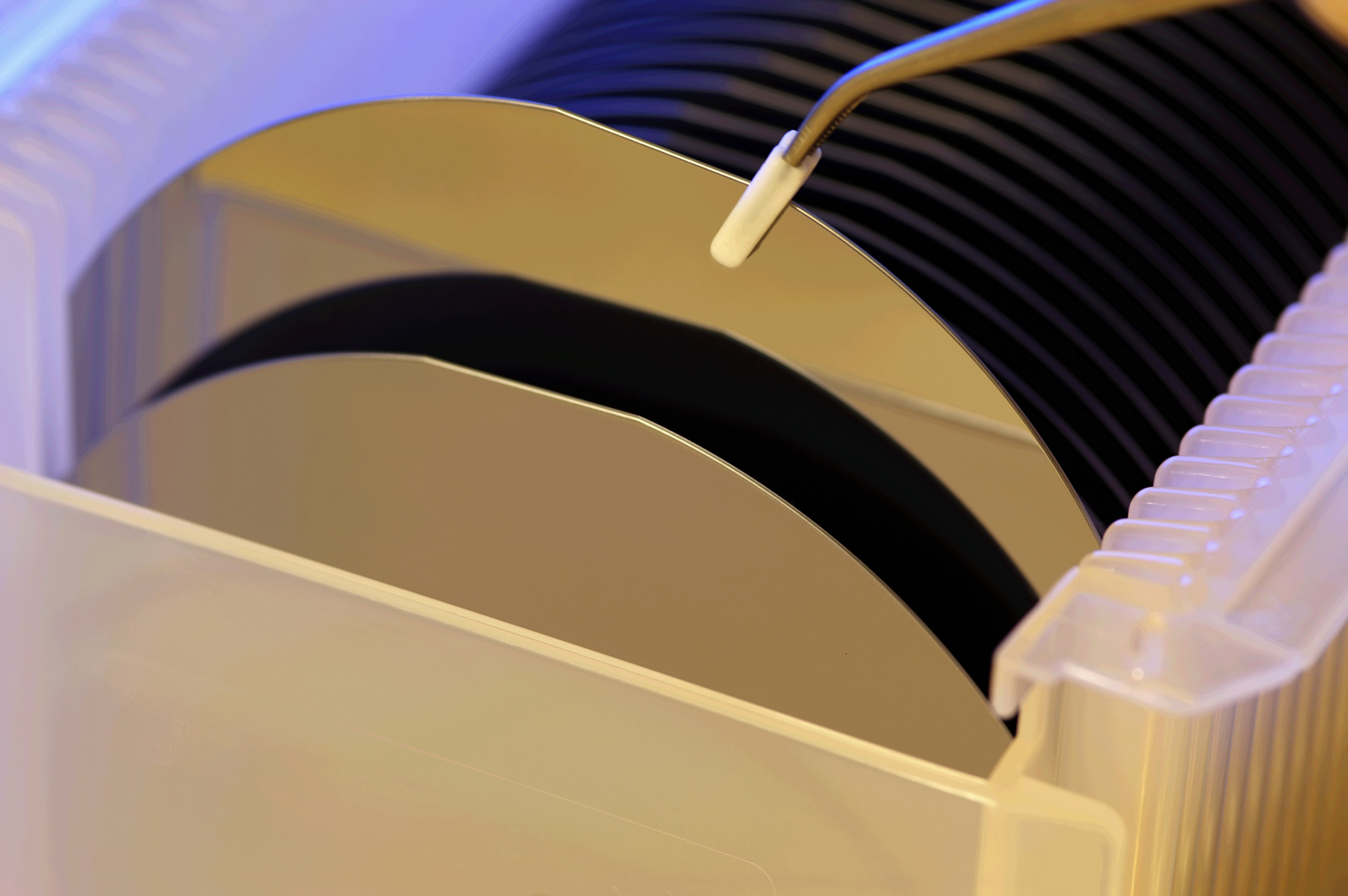
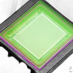
They have developed the first 3D stack imager at a 1.44µm pitch using wafer-to-wafer direct hybrid technology.
Séverine Chéramy, director of IRT Nanoelec’s 3D integration program, said the objective is to demonstrate the value of wafer-to-wafer technologies, using fine-pitch, direct hybrid bonding, for a new use case.